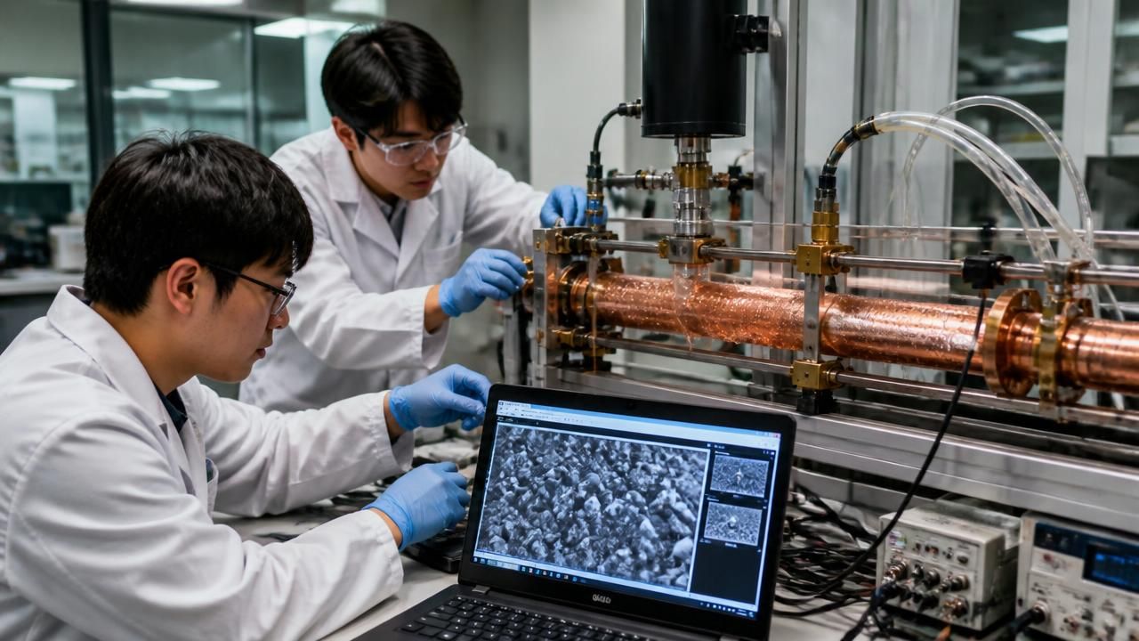
For decades, defects in materials have been viewed as imperfections to be eliminated. But a wave of research is turning that idea on its head, showing that flaws—from nanoscale wrinkles to polymer bumps—can be engineered to dramatically improve performance. The latest breakthrough comes from KAIST, where scientists have developed an ultrathin coating that exploits surface defects to boost heat transfer during condensation by up to 5.5 times compared to conventional copper.
The findings, reported in Science Daily and bioengineer.org, describe a surface where tiny polymer structures—once dismissed as defects—serve as nucleation sites for water droplets. More importantly, the coating helps those droplets detach rapidly, exposing fresh areas for condensation and creating a self-sustaining cycle of heat exchange. In tests on copper tubes, the treated surface transferred heat 5.5 times more effectively than bare copper and more than 50% better than a standard water-repelling coating.
A serendipitous discovery
The research team at the Korea Advanced Institute of Science and Technology (KAIST) initially set out to create a smooth, hydrophobic surface. Instead, they noticed that random polymer bumps—the kind usually considered fabrication errors—were actually improving droplet formation. “We realized that these defects were not just harmless; they were beneficial,” said one researcher. By carefully controlling the size and spacing of these microstructures, the team maximized both droplet nucleation and removal, a dual effect that has eluded previous designs.
The coating’s ultrathin profile means it could be applied to existing heat exchangers, power plants, and cooling systems with minimal added weight or volume. The implications for energy efficiency are enormous, since condensation is a critical step in many industrial processes, from desalination to HVAC systems.
Defects as a theme across materials science
The KAIST result is not an isolated curiosity. Across different fields, researchers are discovering that defects can be harnessed rather than feared.
Electronics and computing
A separate study highlighted by ScienceDaily found that “flaws make electronics faster, smarter, and more efficient.” In microelectronics, tiny defects known as oxygen vacancies can actually enhance the performance of transistors and memory devices by enabling better charge transport. Meanwhile, researchers at Argonne National Laboratory are using physics-informed artificial intelligence to predict how these defects affect microelectronic performance, allowing engineers to design chips that leverage imperfections for speed and energy savings.
But not all defects are helpful. MIT researchers reported that a tiny wrinkle in a chip can trap heat and reduce conductivity by five times, a cautionary tale for chip designers. This dichotomy underscores the need for precise control—defects are neither universally good nor bad; their impact depends on context.
Additive manufacturing
In 3D printing, a study on nano-scale metallic parts found that these structures are surprisingly strong despite containing numerous defects. The high surface-to-volume ratio and the way defects are distributed at small scales can actually block dislocation motion, making the material stronger than bulk metals with fewer imperfections. This challenges the traditional strength-ductility trade-off and opens new avenues for lightweight, robust components in aerospace and biomedical devices.
Optics and thermoelectrics
Researchers at the University of Illinois reported a method to “turn off backscattering” in optical waveguides, using engineered defects to guide light more efficiently. In thermoelectrics, MIT scientists are exploring ways to “turn heat into electricity” by introducing defects that scatter phonons (heat carriers) while allowing electrons to pass, improving conversion efficiency. This approach could make waste-heat recovery a viable power source.
Fundamental physics
Even at the most basic level, defects are reshaping our understanding of materials. In a surprising twist, ScienceDaily reported that graphene—a material known for its perfect lattice—can defy a fundamental law of physics when defects are introduced. While the details are still under investigation, the result suggests that defects can alter not just material properties, but the very rules that govern them.
From radiation damage to heat management
Another study, published in Science, visualized ultrafast melting initiated from radiation-driven defects in solids. By bombarding a crystal with high-energy particles, researchers created localized defects that act as melting nucleation points, allowing the phase transition to occur far more quickly than in a perfect lattice. This has implications for designing radiation-resistant materials for nuclear reactors and space applications.
Broader implications and outlook
The convergence of these findings signals a paradigm shift in materials science. Instead of attempting to create flawless materials, engineers are learning to design defects with purpose—sometimes called “defect engineering.” From boosting heat transfer in industrial systems to making electronics faster and 3D-printed parts stronger, the power of imperfection is becoming a central tool for innovation.
“Defects are no longer just a nuisance to be eliminated. They are a design parameter,” said a materials scientist from an another institution, summarizing the sentiment.
As research continues, the challenge will be to develop fabrication methods that precisely control defect size, density, and location. The KAIST coating is a step in that direction, offering a practical demonstration of how microscopic flaws can deliver macroscopic performance gains. With energy efficiency becoming a global priority, such defect-driven solutions could play a key role in reducing heat-related losses across industries.
The next decade will likely see more examples of scientists turning “problems” into opportunities, proving that in the world of materials, perfection is overrated.