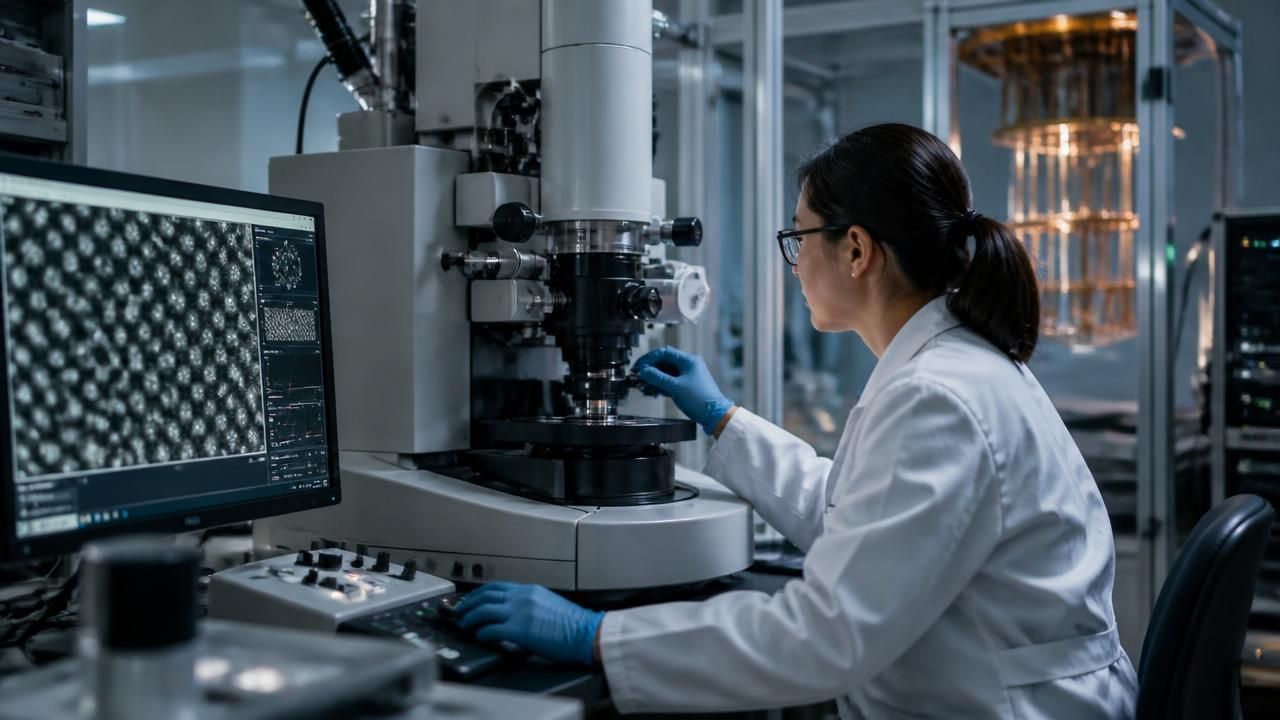
Two normally separate corners of physics — quantum computing and electron microscopy — are converging in a set of instrument advances that researchers say could change how scientists image everything from biological tissue to the transistors inside a microchip.
At the center of the convergence is a simple problem: electron microscopes are extraordinarily powerful, but they work by firing charged particles at a sample. That beam can alter or destroy the very thing being examined, particularly soft biological specimens and delicate quantum materials. Researchers are now betting that quantum hardware — both computational and sensing — can extract more information from each electron, or read a sample's properties without touching it at all.
Fewer electrons, more information
One strand of work combines an electron microscope with a quantum computer, according to reporting by Science Daily. The goal is not simply to speed up image processing but to fundamentally change the information economics of microscopy: if a quantum processor can wring more signal out of every electron detection event, researchers can use fewer electrons and deliver lower doses to the specimen.
The approach could reveal faint details with fewer electrons, helping protect fragile samples that conventional microscopy can damage.
That framing matters. In conventional electron microscopy, the trade-off between resolution and damage is a hard limit that has shaped experimental design for decades. Cryogenic freezing, low-dose imaging techniques, and averaging across many identical samples have all been developed to work around it. A quantum-assisted readout would attack the problem at its source rather than compensating for it downstream.
A quantum computer you can plug into a wall
The second strand is about accessibility. As reported by MSN, engineers have built what is described as the world's first portable, diamond-powered quantum computer — one that operates at room temperature and can be plugged into an ordinary electrical outlet.
That specification is the headline. Most leading quantum computing platforms — superconducting circuits, trapped ions — require elaborate cryogenic systems that cool hardware to near absolute zero, along with laser arrays, vacuum chambers, and racks of control electronics. Portability has therefore been treated as a distant aspiration rather than a near-term design goal.
Diamond-based systems sidestep this. They exploit defects in diamond — notably nitrogen-vacancy centers — whose electron spins can be manipulated and read out optically, and which retain their quantum properties at ambient temperature. The same physics underpins a growing family of quantum sensors: devices that use spin states to measure magnetic fields, electric fields, temperature, and strain with extreme sensitivity.
The microscope that looks inside a transistor
That sensing capability is where the third thread runs, with phys.org reporting on a quantum sensing microscope designed to illuminate transistor design. Rather than imaging a chip's surface with electrons, a quantum sensor can map the magnetic fields generated by current flowing through a device — effectively watching a transistor work in real time, and exposing defects, hot spots, and leakage paths that conventional inspection struggles to localize.
The industrial stakes are considerable. As semiconductor manufacturers push into three-dimensional architectures, gate-all-around transistors, and advanced packaging, the ability to characterize devices non-destructively and at nanometer scale becomes a bottleneck on iteration speed. A tool that reveals what is happening inside a working transistor — not a cross-section of a sacrificed one — would compress design cycles and improve yield analysis.
Three framings, one story
The sources frame the same underlying trend quite differently. Science Daily emphasizes scientific capability and sample preservation — a research-community story about what becomes measurable. The MSN report frames it as an engineering and accessibility milestone, emphasizing room-temperature operation and the plug-into-a-wall practicality. The phys.org headline points toward industrial application, positioning quantum sensing as a tool for transistor designers rather than laboratory physicists.
Each framing reflects a distinct audience and a distinct set of expectations about what quantum technology is for: discovery, democratization, or manufacturing.
Why it matters now
- Gentler imaging: Lower electron doses could open fragile biological and quantum-material samples to high-resolution study.
- Deployment outside the lab: Room-temperature, outlet-powered quantum hardware suggests sensing applications in factories, hospitals, and field settings.
- Semiconductor metrology: Quantum magnetic imaging offers a non-destructive window into working chips at a moment when device complexity is rising fast.
Important caveats remain. Details on performance, cost, and scaling for both the quantum-enhanced microscope and the portable diamond computer are still sparse in the public reporting, and the gap between a working demonstration and a commercially useful instrument is often measured in years. Quantum-enhanced measurement also demands careful error characterization — a sensor that is exquisitely sensitive to a transistor's magnetic field is, by design, sensitive to noise as well.
Still, the direction of travel is clear. Quantum technology's first broad impact may not arrive as a machine that breaks cryptographic codes or simulates molecules on demand. It may arrive as a set of instruments — microscopes, magnetometers, sensors — that let researchers see what existing tools cannot, and that fit on a bench beside the equipment they are meant to improve.